Semiconductor nanostructures
Summary
We develop and use methods for analysis of nanostructures with highest possible spatial and temporal resolution. One aim of this research is to understand the role of the surfaces and interfaces for their function and properties. Another goal is to study devices under as realistic conditions as possible. The aim is both fundamental physical understanding as well as enabling the design of novel devices. We study primarily semiconductors for light-emitting diodes, solar cells, low-energy electronics, and computation.
To this end, we use a wide range of X-ray methods at different synchrotrons, including MAX IV in Lund as well as ESRF and PETRA-III, ultrafast lasers at Lund Laser Centre, and a variety of high resolution scanning probe microscopes maintained by our division, including Sweden’s largest facility for scanning tunneling microscopy. We collaborate with many other researchers in particular within NanoLund, elsewhere at Lund University, and internationally.
Imaging atomic scale structure, dynamics and electronic properties

Direct access to electronic and geometric structure of solid surfaces to the Ångström length scale is available uniquely by Scanning Tunneling Microscopy. Probing even down to individual atoms on functional nanostructure materials is relevant as just one impurity in one specific location can have significant influence on physical properties. Uniquely we can probe even atomic scale defects inside and outside of semiconductor nanowires. This will be used for rational design of novel low dimensional atomic scale structures as well as investigating how atomic scale structures fundamentally respond to electronic or optical signals.
Contact
Anders Mikkelsen's contact information in Lund University's Research Portal
Operando investigation of nanodevices using scanning probe microscopy

We want to bridge the gap between surface characterization (typically done on ideal model surfaces) and device processing, by investigating semiconductor nanostructures during device operation at the atomic scale. We use scanning tunneling microscopy and atomic force microscopy in different newly developed setups for operando surface studies of technologically relevant nanostructure devices.
Contact
Rainer Timm's contact information in Lund University's Research Portal
Ultrafast nanostructure imaging
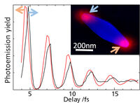
A nanostructure only becomes relevant through its function -inherently a dynamic process. Light travels the typical distance between atoms in solids (~3 Ångström) in one attosecond. This indicates that attosecond and femtosecond timescales can be relevant for structures confined to the (sub-) nanometer scale in one or more dimensions. We combine the extreme time resolution of cutting edge laser technology with the extreme spatial resolution of electron emission and tunneling microscopes. A central goal is to obtain new insights into fundamental concepts such as electron screening, scattering, tunneling, coherence and excitation in low dimensional compound semiconductor and metal (nano) structures. These studies are done in tight collaboration with researchers at Lund Laser Centre (LLC).
Contact
Anders Mikkelsen's contact information in Lund University's Research Portal
X-ray-based spectroscopy of nanostructure devices

We apply X-ray photoelectron spectroscopy in order to obtain chemical information from nanostructure surfaces and interfaces and correlate it with atomic-scale structural and electronic properties. We want to know how local surface and interface composition influences device performance, therefore we study individual nanostructure devices during operation, and we follow chemical surface reactions in-situ.
Contact
Rainer Timm's contact information in Lund University's Research Portal
X-ray detection and X-ray induced current in nanostructures
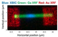
In this project, nanofocused X-rays are used for local excitation of semiconductor nanowires. The X-rays generate electron-hole pairs, which can be measured as an electric current. We use this process, called X-ray beam induced current (XBIC), to locally probe the diffusion lengths and electric fields. The process can also be used for X-ray detection with very high spatial resolution.
Contact
Jesper Wallentin's contact information in Lund University's Research Portal
Interested in working with us?
Available BSc/Msc projects
We welcome candidates for BSc and MSc thesis.
PhD and PostDoc positions
When available published on Lund University's website. Direct contact is welcome.